Conceptual Applications of Semiconductors, Wafers, Iithography, Chips, and Integrated Circuits
Starting with semiconductors, semiconductors are substances with conductivity between conductors (metals) and insulators (stones), including silicon and germanium. Due to the large gaps in silicon that can be doped with impurities, it can be used to manufacture important semiconductor electronic components - transistors. The main functions of transistors are to amplify signals and switches. Transistors are like data signal radios. The principle of radios is to amplify weak signals and use speakers to release them, while transistors can amplify the current of signals, allowing current to pass through in a specific way.
Hundreds of millions of transistors are installed on a chip about half a centimeter in length and width. This chip is commonly known as an 'integrated circuit', commonly known as an IC (Integrated Circuit). Therefore, a chip is the abbreviation of an integrated circuit, also known as a carrier.
The following article will be divided into four main parts:
- Semiconductor manufacturing process: 4 major steps
- Classification of integrated circuits: four major categories for functional differentiation
- Semiconductor Industry Chain Operation Models: Advantages and Disadvantages of Various Models
- Semiconductor application fields: 6 major areas for future applications
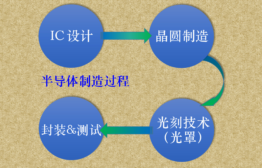
Semiconductor manufacturing process: 4 major steps
1. IC design:
The functions of the chip are planned in advance, including arithmetic logic, memory function, floating point operation and data transmission. Each function is distributed in each area of the chip, and the required electronic components are produced. The engineers use hardware description language (HDL) to design the circuit diagram. When the HDL program code is put into the EDA Tool, the computer converts the program code into the circuit diagram.
2. Wafer manufacturing:
Purify and dissolve silicon into a liquid state, and pull it into a columnar silicon crystal column. There are grid by grid silicon lattices on top, and place transistors on the silicon lattice. The arrangement of the silicon lattice is an important key to installing electronic components. The speed and temperature at which the silicon crystal column is pulled up affect the quality of the silicon crystal column. The larger the size, the higher the technical difficulty. The 12 inch wafer factory is also more advanced than the 8 inch wafer factory in the process, which is technology, But yield is the most crucial knowledge. Wafer factories use diamond knives to cut the entire silicon crystal column into thin slices, which are then polished to become 'wafers', which are the boards of the chips. Dust poses a serious threat to these wafers. Therefore, before entering the clean room, manufacturing personnel need to wear dustproof clothing, clean their bodies, and take preventive measures. Wafer manufacturing is 100000 times cleaner than the operating room.
3. Lithography production (mask):
A large circuit design diagram, scaled down and stamped onto a silicon wafer, relies on optical principles.
The IC design diagram is etched onto a quartz chip using an electron beam to form a mask. The design diagram on the mask is reduced to a wafer, similar to the principle of photo development. The "mask" is like a photographic film, while the "wafer" is like photo paper. The wafer is coated with a layer of photoresist (photo sensitive material) in advance, and the circuit structure on the mask is reduced and imprinted on the wafer through ultraviolet light irradiation and convex lens focusing effect, The precision of the graphics on the mask is the key to affecting the quality of the chip.
After the photolithography process is completed, engineers add ions to the wafer and control conductivity and a series of physical processes by injecting impurities into the silicon structure, creating transistors. After the production of electronic components such as transistors and diodes on the wafer is completed, copper is poured into the grooves to form precise wiring, connecting many transistors together.
4. Packaging and testing:
After the wafer is completed, it is sent to the packaging factory and cut into bare crystals one by one. Due to the small and thin size of the bare crystals, they are very easy to scratch. Therefore, the bare crystals are installed on the wire rack, with an insulated plastic or ceramic shell on the outside, printed with the logo of the commissioned manufacturing company. Finally, chip testing is carried out to pick out defective products, and the chip is completed.
Classification of Integrated Circuits (ICs): Four major categories by function
1. Memory IC:
Mainly used to store original documents,
Commonly used in computers, TV games, electronic dictionaries, and so on. DRAM, SRAM, NAND Flash are all memory ICs.
2. Logic IC:
Mainly processing digital signals (0 and 1), the product includes a central processing unit (CPU), a microprocessor (MPU), and a graphics processor (GPU).
3. Microelement IC:
The main function is to be responsible for communication tasks with peripheral devices and other components of the CPU, skilled in handling complex logical operations, mainly digital or textual data.
4. Analogy IC:
Mainly processing IC related to analog signals, it is mainly used in power supplies, digital analog converters, etc. due to its ability to withstand high voltage and high current. The semiconductor industry chain operation mode: the advantages and disadvantages of various modes. Early semiconductor companies mostly handled IC design, manufacturing, packaging, and testing all at once. Due to Moore's Law, chip design became increasingly complex and expensive, A single semiconductor company was unable to bear the high R&D and production costs from upstream to downstream. By the end of 1980, the semiconductor industry gradually moved towards a professional division of labor model, creating greater profits and improving product stability.
※ Moore's Law:According to Gordon Early Moore, one of the founders of Intel, the number of transistors that can be accommodated on an integrated circuit will double approximately every 18 months, and the performance will also double.
According to the nature of business, the semiconductor industry is mainly divided into the following four business models:
1. Integrated Manufacturer (IDM) Mode:
Integrating multiple industry chain links such as chip design, manufacturing, packaging, testing, and sales requires strong working capital to support this operating model, so currently only a few large factories can sustain it.
Advantages: a. Optimization in design, manufacturing, etc. b. Able to experiment and promote new technologies first
Disadvantage: High operating costs
Representative: Samsung, Intel
2. Foundry mode:
We only need to be responsible for manufacturing, packaging, and testing, and can serve multiple design manufacturers at the same time. However, due to supplier competition, we need to pay special attention to the leakage of customer confidential technology. The main competitiveness of the OEM factory comes from large-scale production and production control.
Advantages: a. Does not bear risks such as circuit design or product sales. b. Profits are relatively stable
Disadvantages: a. Relying on physical assets and having a high demand for funds; b. requiring a large amount of capital to maintain the level of craftsmanship
Representatives: TSMC, Liandian, Sunrise, and Sipin
3. Fabless mode:
Responsible only for chip circuit design and sales, outsourcing production, packaging, and testing. Initially, the funding scale was not large, and the entry threshold was relatively low.
Advantages: a. No large physical assets, small founding scale b. Low operating costs for the enterprise
Disadvantages: a. Unable to achieve upstream and downstream integration b. Need to shape the brand and bear sales risks
Representatives: Qualcomm, MediaTek
4. Chip Design Service Provider Mode:
To provide chip design companies with corresponding tools, circuit design architecture, consulting services, etc. Instead of designing and selling chips, they sell intellectual property rights - design drawings, also known as silicon intellectual property (SIP).
Advantages: a. No large physical assets, small scale b. No need to bear sales risk
Disadvantages: a. Easy to form monopolies; b. High technical threshold and long cumulative technical time
Representatives: ARM, Xinsi Technology, Imagination
Semiconductor application fields: 6 major areas for future applications
According to the International Semiconductor Industry Association, semiconductors will mainly be used in smart transportation, smart healthcare, smart data, smart manufacturing, green manufacturing, and advanced manufacturing in the future. And transportation and industrial manufacturing are the two main driving forces. The level of intelligent vehicle driving assistance safety system is getting higher and higher. Through the backend AI chip calculation, the sensing signal is received, analyzed, and then transmitted to the vehicle power system, which can meet the requirements of safe avoidance and reaching the destination, achieving the vision of fully automated driving. Industrial manufacturing has evolved from digitalization to fully automated production, introducing IoT systems into production management systems, promoting a new era of industrial intelligent manufacturing and driving overall semiconductor market demand.
In the future, 5G, AI, and the semiconductor industry are closely related. The arrival of the 5G era will drive the entire semiconductor peripheral goods. For example, the demand for nearly 200 million units in the 5G smart phone market will bring another wave of device switching. AI intelligence requires a large amount of computing efficiency to constantly innovate wafer technology to adapt to rapid technological changes, and the semiconductor industry is expected to reach another peak in the future.